
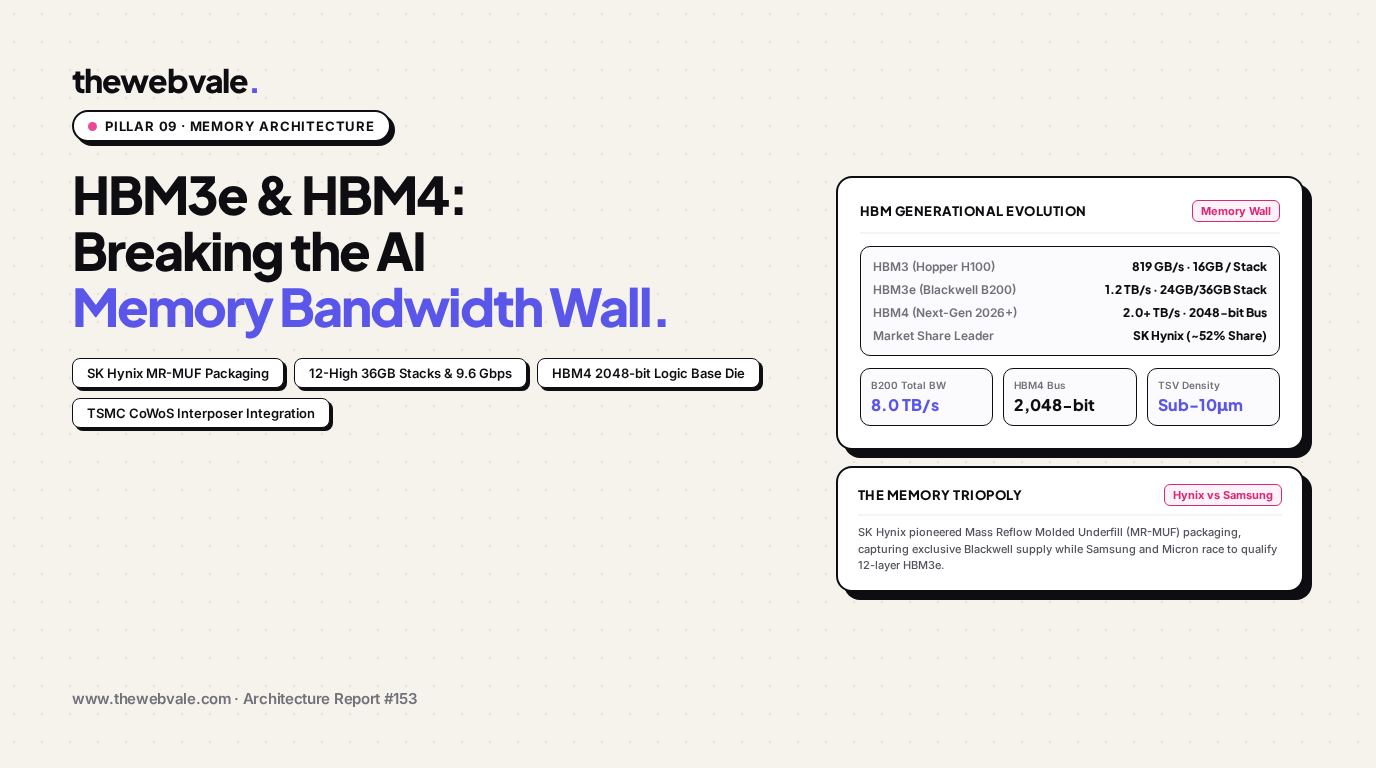
High Bandwidth Memory (HBM3e/HBM4): SK Hynix, Samsung, Micron & The Memory Bandwidth Wall
In the computational hierarchy, processing power without memory bandwidth is an empty illusion. Over the last decade, AI accelerators achieved an astounding 1,000x increase in raw floating-point operations per second (FLOPs). Yet over that identical decade, standard DDR and GDDR memory bandwidth expanded by less than 20x.
This stark divergence represents the single most critical bottleneck in computer architecture: the Memory Wall. In autoregressive language model inference and massive parameter sharding, processors spend the overwhelming majority of their clock cycles waiting for weights to travel across memory buses. To break this barrier, the semiconductor industry abandoned planar printed circuit board (PCB) traces and pioneered High Bandwidth Memory (HBM)—stacking dynamic random-access memory (DRAM) dies vertically in three dimensions using microscopic Through-Silicon Vias (TSVs). In this report, we dissect the physics of HBM3e, the competitive battle between SK Hynix, Samsung, and Micron, and the upcoming architectural leap to HBM4.
Silicon Schematic: 12-High HBM3e 3D Stack on CoWoS Silicon Interposer
Cross-sectional view: 12 vertically stacked DRAM dies with Through-Silicon Vias (TSVs), microbump interconnects, base buffer logic die, and passive silicon interposer link to GPU ASIC.
1. Architecture of 3D Vertical Stacking: TSVs and Microbumps
Traditional GDDR6X memory (used in consumer cards like the RTX 4090) communicates over wide PCB copper traces limited to 384 bits. Because signal integrity degrades rapidly over long physical distances, memory chips must be placed around the perimeter of the processor, limiting memory bandwidth to approximately 1,000 GB/s.
High Bandwidth Memory fundamentally changes the physical geometry by moving memory onto the same packaging substrate as the GPU:
- Substrate Thinned to Microns: Individual DRAM wafers are mechanically polished and chemical-mechanically planarized until the silicon wafer thickness is reduced to under 40 microns (thinner than a human hair).
- Through-Silicon Vias (TSVs): Tens of thousands of vertical holes (measuring ~5 microns in diameter) are etched through each DRAM layer using reactive-ion etching and filled with electroplated copper.
- Microbump Interconnects: Microscopic solder bumps with a pitch of just 25 to 35 microns bond the stacked dies vertically. In a 12-high HBM3e stack, over 60,000 individual electrical connections link the 12 DRAM layers to the base logic buffer die, operating an ultra-wide 1024-bit parallel bus.
2. The Manufacturing War: SK Hynix MR-MUF vs. Samsung TC-NCF
While three firms compose the global memory triopoly—SK Hynix, Samsung Electronics, and Micron—SK Hynix emerged as the undisputed king of AI memory, capturing over 50% to 55% global HBM market share and securing near-total allocation on NVIDIA's H100 and B200 platforms.
The key to SK Hynix's dominance is packaging physics:
A. Samsung's Traditional Approach: TC-NCF
Samsung utilized Thermal Compression Non-Conductive Film (TC-NCF). Before stacking each DRAM die, a solid film layer is placed between the chips. A thermal head applies high heat and pressure to melt the microbumps and bond the film. However, as stacks increased from 8 layers to 12 layers, TC-NCF suffered from silicon warpage, micro-void formation, and poor thermal dissipation, leading to yield issues that delayed Samsung's qualification with NVIDIA.
B. SK Hynix's Breakthrough: MR-MUF
SK Hynix pioneered Mass Reflow Molded Underfill (MR-MUF):
- All 12 DRAM dies are stacked simultaneously over microbumps without intermediate film, and passed through a single reflow oven to bond all joints in one thermal cycle.
- Next, a liquid epoxy molding compound containing silica fillers is injected under vacuum between the dies.
- 2.5x Higher Thermal Conductivity: The epoxy compound has a thermal conductivity 2.5 times higher than non-conductive film, dissipating GPU heat dramatically faster and preventing thermal expansion defects.
3. Micron's Leapfrog Strategy (1-beta Node)
US memory maker Micron Technology skipped standard HBM3 entirely and leapfrogged directly to HBM3e. Fabricated on its cutting-edge 1-beta (1β) DRAM node using advanced DUV immersion multi-patterning, Micron achieved a pin speed of 9.2 Gbps and 24GB capacity per 8-high stack. By achieving 30% lower power consumption than competitors, Micron secured a critical secondary supply allocation on NVIDIA's H200 and Blackwell platforms.
4. The HBM4 Revolution: 2048-Bit Bus & Custom TSMC Logic Base Dies
Beginning in 2026, the industry transitions to HBM4, marking the most radical architectural redesign in HBM history:
- Doubling the Bus Width to 2048-bit: Standard HBM from version 1 through HBM3e remained locked to a 1024-bit interface. HBM4 doubles the interface to a massive 2,048-bit bus, exceeding 2.0 to 3.0 Terabytes/sec per memory stack. An 8-stack GPU using HBM4 will command over 16 to 24 TB/s of aggregate memory bandwidth.
- The End of the DRAM Base Die: In HBM3e, the bottom "base die" is fabricated on trailing-node memory processes. In HBM4, the base die is a custom advanced logic die fabricated on TSMC's 3nm or 5nm process node.
- Co-Design with GPU Silicon: Because the HBM4 base die is manufactured on pure logic silicon, memory makers can embed near-memory computing, hardware encryption, and custom PHY interfaces co-designed directly with NVIDIA, Apple, and AMD architectures.
5. Comprehensive HBM Generational Matrix
| HBM Generation | Bus Width | Pin Speed | Per-Stack Bandwidth | Max Capacity (Stack) | Representative GPU Platform |
|---|---|---|---|---|---|
| HBM2e | 1024-bit | 3.2 – 3.6 Gbps | 410 – 460 GB/s | 16 GB (8-Hi) | NVIDIA A100 (80GB) |
| HBM3 | 1024-bit | 6.4 Gbps | 819 GB/s | 16 – 24 GB (8-Hi) | NVIDIA H100 SXM5 |
| HBM3e (8-High) | 1024-bit | 8.0 – 9.2 Gbps | 1,024 – 1,177 GB/s | 24 GB (8-Hi) | NVIDIA H200 · GH200 |
| HBM3e (12-High) | 1024-bit | 9.6 Gbps | 1,228 GB/s (1.2 TB/s) | 36 GB (12-Hi) | NVIDIA Blackwell B200 (192GB) |
| HBM4 | 2048-bit (2x Bus) | 10.0+ Gbps | > 2,000 – 3,000 GB/s | 48 – 64 GB (16-Hi) | NVIDIA Rubin (2026/2027) |
6. Production Simulation: Memory Bandwidth Roofline & Decode Latency Simulator
The Python script below models the autoregressive token generation throughput of a 70B parameter model across HBM generations, illustrating the exact speedup from HBM2e to HBM4:
# -*- coding: utf-8 -*-
"""
TheWebVale Silicon Lab — HBM Memory Bandwidth & Token Generation Simulator
Quantifies the exact autoregressive decode bottleneck across HBM2e, HBM3, HBM3e, and HBM4.
"""

import dataclasses
from typing import Dict

@dataclasses.dataclass(frozen=True)
class MemorySubsystem:
    generation: str
    num_stacks: int
    bandwidth_per_stack_gb_s: float
    capacity_per_stack_gb: float

    @property
    def total_bandwidth_tb_s(self) -> float:
        return (self.num_stacks * self.bandwidth_per_stack_gb_s) / 1000.0

    @property
    def total_capacity_gb(self) -> float:
        return self.num_stacks * self.capacity_per_stack_gb

def model_llm_inference_speed(
    memory: MemorySubsystem,
    model_param_count_b: float,
    bytes_per_param: float = 2.0  # FP16 = 2 bytes
) -> Dict[str, float]:
    """
    At Batch=1, token generation is memory-bandwidth bound:
    Throughput (tok/s) = Total Bandwidth (GB/s) / Model Size (GB)
    """
    model_size_gb = model_param_count_b * bytes_per_param
    total_bw_gb_s = memory.total_bandwidth_tb_s * 1000.0

    # Check if model fits in memory
    fits_in_memory = memory.total_capacity_gb >= model_size_gb
    theoretical_tok_per_sec = (total_bw_gb_s / model_size_gb) if fits_in_memory else 0.0

    return {
        "hbm_generation": memory.generation,
        "total_bandwidth_tb_s": round(memory.total_bandwidth_tb_s, 2),
        "total_capacity_gb": memory.total_capacity_gb,
        "model_size_gb": model_size_gb,
        "fits_in_vram": fits_in_memory,
        "batch1_throughput_tokens_per_sec": round(theoretical_tok_per_sec, 1)
    }

if __name__ == "__main__":
    hbm_configurations = [
        MemorySubsystem("HBM2e (6x Stacks - A100)", num_stacks=6, bandwidth_per_stack_gb_s=338.0, capacity_per_stack_gb=13.3),
        MemorySubsystem("HBM3 (6x Stacks - H100)", num_stacks=6, bandwidth_per_stack_gb_s=558.0, capacity_per_stack_gb=13.3),
        MemorySubsystem("HBM3e (8x Stacks - B200)", num_stacks=8, bandwidth_per_stack_gb_s=1000.0, capacity_per_stack_gb=24.0),
        MemorySubsystem("HBM4 (8x Stacks - Rubin)", num_stacks=8, bandwidth_per_stack_gb_s=2500.0, capacity_per_stack_gb=36.0)
    ]

    target_model_params = 70.0 # 70 Billion parameter model (140 GB in FP16)

    print(f"=== 70B FP16 MODEL (140 GB) DECODING SPEED ACROSS HBM GENERATIONS ===")
    for mem in hbm_configurations:
        res = model_llm_inference_speed(mem, target_model_params, bytes_per_param=2.0)
        status = f"{res['batch1_throughput_tokens_per_sec']} tok/s" if res['fits_in_vram'] else "OOM (Insufficient VRAM)"
        print(f"[{res['hbm_generation']:<32}] BW: {res['total_bandwidth_tb_s']:>4.1f} TB/s | Capacity: {res['total_capacity_gb']:>3.0f} GB | Speed: {status}")
7. Summary: Memory as the Ultimate Arbiter of AI Supremacy
The battle for artificial intelligence leadership is fundamentally a battle for high-bandwidth memory. As models scale and test-time reasoning multiplies inference token volumes, the speed at which weights can be streamed from DRAM into compute logic determines application latency and total datacenter cost of ownership. The companies that master 3D packaging, Through-Silicon Via reliability, and custom logic base die integration will dictate the cadence of machine learning progress for the decade ahead.